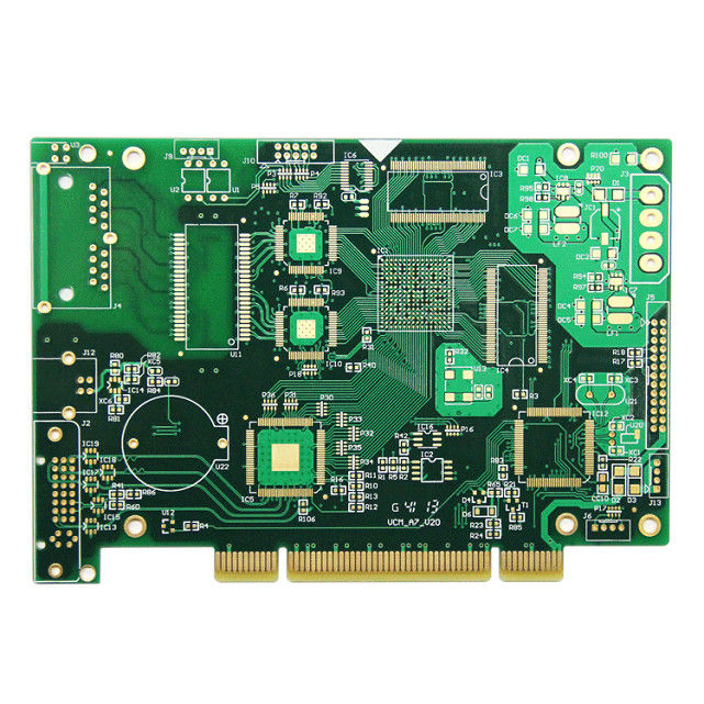

6 layer blind hole PCB Prototype FR4 pcb board Gold finger PCB
6 layer fr4 pcb board with bilnd hole
1. ONE-STOP-SERVICE
2. OEM service
3. Gerber file needed
4. PCB clone with sample
5. Quality guarantee and professional after-sell service
Our Production Capability for PCB / PWB
Layer: 1 to 18 layers
Material type: FR-4, CEM-1, CEM-3, High TG, FR4 Halogen Free, Rogers
Board thickness: 0.21mm to 7.0mm
Copper thickness: 0.5 OZ to 7.0 OZ
Copper thickness in hole: >25.0 um (>1mil)
- Max. Board Size: 23 × 25 (580mm×900mm)
- Min. Drilled Hole Size: 3mil (0.075mm)
- Min. Line Width: 3mil (0.075mm)
- Min. Line Spacing: 3mil (0.075mm)
Surface finishing: HASL / HASL lead free, HAL, Chemical tin, Chemical Gold, Immersion Silver/Gold, OSP, Gold plating
Solder Mask Color: Green/Yellow/Black/White/Red/Blue
Tolerance
- Shape tolerance: ±0.13
- Hole tolerance: PTH: ±0.076 NPTH: ±0.05
PCB Packing
- Inner packing: Vacuum packing / Plastic bag
- Outer packing: Standard carton packing
Certificate: UL, ISO 9001, ISO 14001
Special requirements: Buried and blind vias+controlled impedance +BGA
Profiling: Punching, Routing, V-CUT, Beveling
Provides OEM services to all sorts of printed circuit board assembly as well as electronic encased products.
PCB Capacity
|
Item |
Capability---Technology |
|
Standard |
IPC-A-610 E Class II-III |
|
Laminate/Base Material |
FR-4 / PI (FPC) / High TG FR-4 / Halogen Free material/Rogers/Arlon/ Taconic/Teflon/CEM-3/PTFE/Aluminum /BT |
|
Layers |
1-18 |
|
Finised inner/outer copper thickness |
1-6 OZ |
|
Board Thinkness |
0.2-5.0mm |
|
Min hole size |
Mechanical hole: 0.15mm |
|
Laser hole: 0.1mm |
|
|
Min line width/space |
0.075mm/0.075mm |
|
Min line Gap |
+/-10% |
|
Aspect Ratio |
12:1 |
|
Controlled Impedance |
<= +/-10% |
|
Solder Mask Color |
Green,Blue,Black,White,Yellow,Red,Grey,Purple etc.. |
|
Outline profile |
Rout/ V-cut/ Bridge/ Stamp hole |
|
Surface treatment |
HASL, HASL lead free, Immersion Gold,ENEPIG, Immersion Tin, Immersion Silver, Hard gold, Flash gold, OSP... |
|
Tolerance of dimension size |
+/-0.1mm |
|
Capacity |
35000sq/Month |
|
CAM Capability |
40 item |
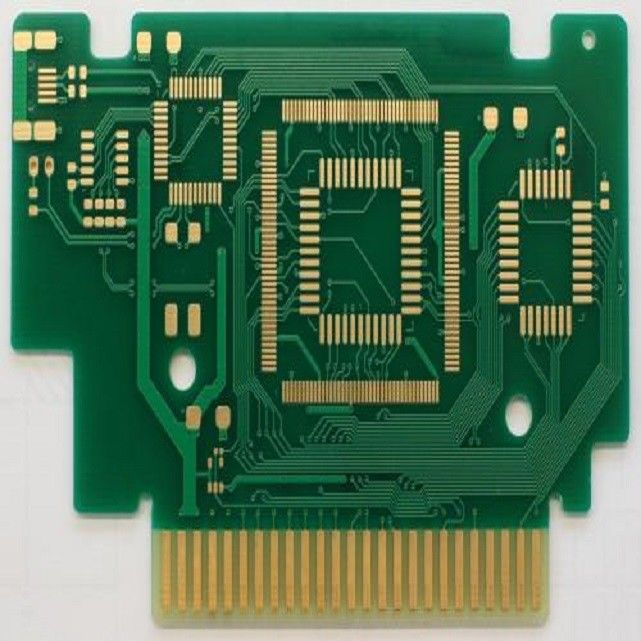
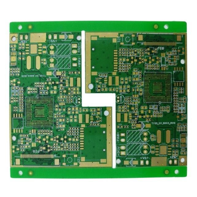
PCB Photos
![]()
![]()
Our products are sold all over the world, you can rest assured.